
12.2.1: Electron Microscopes
- Page ID
- 18390

\( \newcommand{\vecs}[1]{\overset { \scriptstyle \rightharpoonup} {\mathbf{#1}} } \)
\( \newcommand{\vecd}[1]{\overset{-\!-\!\rightharpoonup}{\vphantom{a}\smash {#1}}} \)
\( \newcommand{\dsum}{\displaystyle\sum\limits} \)
\( \newcommand{\dint}{\displaystyle\int\limits} \)
\( \newcommand{\dlim}{\displaystyle\lim\limits} \)
\( \newcommand{\id}{\mathrm{id}}\) \( \newcommand{\Span}{\mathrm{span}}\)
( \newcommand{\kernel}{\mathrm{null}\,}\) \( \newcommand{\range}{\mathrm{range}\,}\)
\( \newcommand{\RealPart}{\mathrm{Re}}\) \( \newcommand{\ImaginaryPart}{\mathrm{Im}}\)
\( \newcommand{\Argument}{\mathrm{Arg}}\) \( \newcommand{\norm}[1]{\| #1 \|}\)
\( \newcommand{\inner}[2]{\langle #1, #2 \rangle}\)
\( \newcommand{\Span}{\mathrm{span}}\)
\( \newcommand{\id}{\mathrm{id}}\)
\( \newcommand{\Span}{\mathrm{span}}\)
\( \newcommand{\kernel}{\mathrm{null}\,}\)
\( \newcommand{\range}{\mathrm{range}\,}\)
\( \newcommand{\RealPart}{\mathrm{Re}}\)
\( \newcommand{\ImaginaryPart}{\mathrm{Im}}\)
\( \newcommand{\Argument}{\mathrm{Arg}}\)
\( \newcommand{\norm}[1]{\| #1 \|}\)
\( \newcommand{\inner}[2]{\langle #1, #2 \rangle}\)
\( \newcommand{\Span}{\mathrm{span}}\) \( \newcommand{\AA}{\unicode[.8,0]{x212B}}\)
\( \newcommand{\vectorA}[1]{\vec{#1}} % arrow\)
\( \newcommand{\vectorAt}[1]{\vec{\text{#1}}} % arrow\)
\( \newcommand{\vectorB}[1]{\overset { \scriptstyle \rightharpoonup} {\mathbf{#1}} } \)
\( \newcommand{\vectorC}[1]{\textbf{#1}} \)
\( \newcommand{\vectorD}[1]{\overrightarrow{#1}} \)
\( \newcommand{\vectorDt}[1]{\overrightarrow{\text{#1}}} \)
\( \newcommand{\vectE}[1]{\overset{-\!-\!\rightharpoonup}{\vphantom{a}\smash{\mathbf {#1}}}} \)
\( \newcommand{\vecs}[1]{\overset { \scriptstyle \rightharpoonup} {\mathbf{#1}} } \)
\(\newcommand{\longvect}{\overrightarrow}\)
\( \newcommand{\vecd}[1]{\overset{-\!-\!\rightharpoonup}{\vphantom{a}\smash {#1}}} \)
\(\newcommand{\avec}{\mathbf a}\) \(\newcommand{\bvec}{\mathbf b}\) \(\newcommand{\cvec}{\mathbf c}\) \(\newcommand{\dvec}{\mathbf d}\) \(\newcommand{\dtil}{\widetilde{\mathbf d}}\) \(\newcommand{\evec}{\mathbf e}\) \(\newcommand{\fvec}{\mathbf f}\) \(\newcommand{\nvec}{\mathbf n}\) \(\newcommand{\pvec}{\mathbf p}\) \(\newcommand{\qvec}{\mathbf q}\) \(\newcommand{\svec}{\mathbf s}\) \(\newcommand{\tvec}{\mathbf t}\) \(\newcommand{\uvec}{\mathbf u}\) \(\newcommand{\vvec}{\mathbf v}\) \(\newcommand{\wvec}{\mathbf w}\) \(\newcommand{\xvec}{\mathbf x}\) \(\newcommand{\yvec}{\mathbf y}\) \(\newcommand{\zvec}{\mathbf z}\) \(\newcommand{\rvec}{\mathbf r}\) \(\newcommand{\mvec}{\mathbf m}\) \(\newcommand{\zerovec}{\mathbf 0}\) \(\newcommand{\onevec}{\mathbf 1}\) \(\newcommand{\real}{\mathbb R}\) \(\newcommand{\twovec}[2]{\left[\begin{array}{r}#1 \\ #2 \end{array}\right]}\) \(\newcommand{\ctwovec}[2]{\left[\begin{array}{c}#1 \\ #2 \end{array}\right]}\) \(\newcommand{\threevec}[3]{\left[\begin{array}{r}#1 \\ #2 \\ #3 \end{array}\right]}\) \(\newcommand{\cthreevec}[3]{\left[\begin{array}{c}#1 \\ #2 \\ #3 \end{array}\right]}\) \(\newcommand{\fourvec}[4]{\left[\begin{array}{r}#1 \\ #2 \\ #3 \\ #4 \end{array}\right]}\) \(\newcommand{\cfourvec}[4]{\left[\begin{array}{c}#1 \\ #2 \\ #3 \\ #4 \end{array}\right]}\) \(\newcommand{\fivevec}[5]{\left[\begin{array}{r}#1 \\ #2 \\ #3 \\ #4 \\ #5 \\ \end{array}\right]}\) \(\newcommand{\cfivevec}[5]{\left[\begin{array}{c}#1 \\ #2 \\ #3 \\ #4 \\ #5 \\ \end{array}\right]}\) \(\newcommand{\mattwo}[4]{\left[\begin{array}{rr}#1 \amp #2 \\ #3 \amp #4 \\ \end{array}\right]}\) \(\newcommand{\laspan}[1]{\text{Span}\{#1\}}\) \(\newcommand{\bcal}{\cal B}\) \(\newcommand{\ccal}{\cal C}\) \(\newcommand{\scal}{\cal S}\) \(\newcommand{\wcal}{\cal W}\) \(\newcommand{\ecal}{\cal E}\) \(\newcommand{\coords}[2]{\left\{#1\right\}_{#2}}\) \(\newcommand{\gray}[1]{\color{gray}{#1}}\) \(\newcommand{\lgray}[1]{\color{lightgray}{#1}}\) \(\newcommand{\rank}{\operatorname{rank}}\) \(\newcommand{\row}{\text{Row}}\) \(\newcommand{\col}{\text{Col}}\) \(\renewcommand{\row}{\text{Row}}\) \(\newcommand{\nul}{\text{Nul}}\) \(\newcommand{\var}{\text{Var}}\) \(\newcommand{\corr}{\text{corr}}\) \(\newcommand{\len}[1]{\left|#1\right|}\) \(\newcommand{\bbar}{\overline{\bvec}}\) \(\newcommand{\bhat}{\widehat{\bvec}}\) \(\newcommand{\bperp}{\bvec^\perp}\) \(\newcommand{\xhat}{\widehat{\xvec}}\) \(\newcommand{\vhat}{\widehat{\vvec}}\) \(\newcommand{\uhat}{\widehat{\uvec}}\) \(\newcommand{\what}{\widehat{\wvec}}\) \(\newcommand{\Sighat}{\widehat{\Sigma}}\) \(\newcommand{\lt}{<}\) \(\newcommand{\gt}{>}\) \(\newcommand{\amp}{&}\) \(\definecolor{fillinmathshade}{gray}{0.9}\)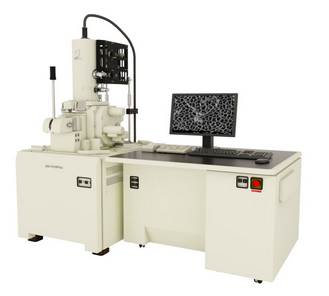
Conventional microscopes use visible light to examine a small specimen, or sometimes a thin section. An electron microscope uses a beam of electrons instead of light. Electron microscopes can magnify samples thousands of times more than conventional light microscopes, allowing us to see very fine mineral grains and details. The greater magnification and resolution are possible because the effective wavelength of an electron is much smaller than the wavelength of light. Consequently, electron optics can focus on much smaller areas than light optics.
There are several different kinds of electron microscopes; scanning electron microscopes (SEMs) are by far the most common. In a scanning electron microscope, such as the one shown in Figure 12.33, high energy (typically 15–20 keV) electrons are generated at the top of the column on the left. The electrons are focused into a narrow beam that scans back and forth (rasters) across a sample at the bottom of the column to produce an image. SEMs can scan very small areas, operating over a wide range of magnifications, up to 250,000x when properly optimized. They can resolve topographical or compositional features just a few nanometers in size. Several different kinds of images can be displayed on a monitor screen depending on the user’s needs.
12.2.1.1 SEM Images
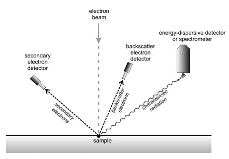
Several important things occur as the electron beam interacts with a sample (Figure 12.34). Some electrons will reflect from the sample surface with no loss of energy. We call these electrons backscatter electrons. Additionally, ionization produces lower-energy secondary electrons when the original high energy electrons interact with valence electrons in the sample. To obtain standard SEM images, a detector measures the intensity of secondary electrons (SE) emitted by the sample as the beam rasters across it. This allows creation of an image with brightness proportional to the number of electrons reaching the detector.
Most SEMs also have a separate detector for creating backscatter electron (BSE) images. For both SE and BSE images, the number of electrons emitted, and thus the brightness or darkness of an image, depends on sample topography and on the composition of the sample. The emission of secondary electrons is particularly sensitive to topography, and only slightly affected by composition. In contrast, the emission of backscatter electrons depends significantly on the composition of the sample. Heavier elements backscatter electrons more efficiently than light elements. So, BSE images show compositional variations within a sample as well as surficial features.
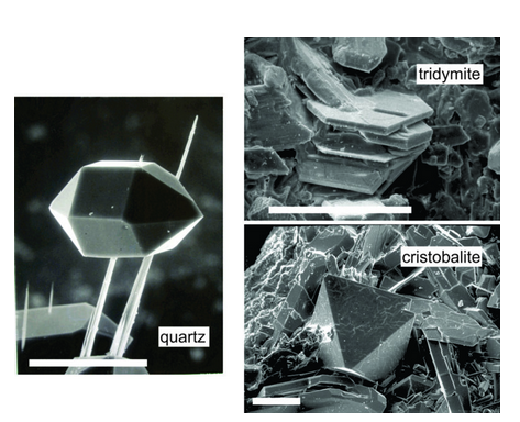
Figure 12.35 shows secondary electron images of very small quartz, tridymite, and cristobalite crystals. These SiO2 polymorphs all belong to different crystal systems and the mineral habits reflect the differences. SE and BSE images, like the images in this figure, sometimes look like conventional photographs but are not the same thing because they do not involve light reflection.
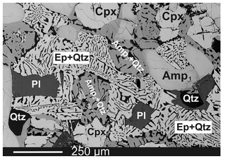
Mineralogists and petrologists sometimes use SEM images to look at rock thin sections. Figure 12.36 shows an example. This is a BSE image of an amphibolite that experienced complex metamorphic reactions. The reactions produced intergrowths of epidote and quartz called symplectites. The very small grains and textures would be hard to see in thin section (the bar scale is 0.25 mm long).
In this image, distinct contrast between white and shades of grey reflect mineral compositions. Dark colored minerals (quartz and plagioclase) are those that contain mostly elements with low atomic numbers. The light colored clinopyroxene and epidote contain significant amounts of heavier elements, in particular iron. The amphibole has an intermediate composition.
12.2.1.2 Secondary X-rays and Characteristic Radiation
An additional important phenomenon occurs when beam electrons hit atoms in a sample. The electrons cause the atoms to emit characteristic secondary X-rays with energy that depends on the element. This process is much the same as the way that the target in an X-ray tube emits X-rays. If the sample contains several different elements, it may emit X-rays at multiple wavelengths corresponding to different energies. Because different elements give off characteristic X-rays with different energies, the emission spectrum displays the chemical composition of the specimen. Most SEMs are equipped with energy-dispersive X-ray detectors for measuring X-ray energies and, thus, for identifying elements in a sample. This analytical method is called energy-dispersive spectroscopy (EDS).
Iron, for example, emits its strongest characteristic radiation (called Kα radiation) at 6.4 keV. So, when struck by a beam of electrons, iron atoms emits energy at 6.4 keV, and the intensity of the emission is proportional to the amount of iron in the specimen. Iron also emits characteristic X-rays of other energies, but the intensities are much less than Kα radiation and rarely used for analysis.
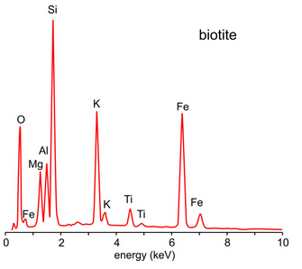
Energy dispersive detectors measure X-ray energy and intensity over a wide range of energies simultaneously. Spectra can be collected quickly, perhaps counting X-rays for just a few seconds, to get an idea of the composition of a sample. For more accurate results, counting times must be longer. Figure 12.37 shows an energy spectrum for biotite. Some elements produced more than one peak but the strongest peak for any element is always Kα. This is a typical spectrum for biotite, but biotite varies in composition so the relative heights of the peaks are not the same for all specimens.
A computer takes a spectrum such as the one in Figure 12.37 and quickly analyzes the intensities of all X-ray peaks to produce an EDS chemical analysis for the sample. EDS analyses are generally semiquantitative, but often that is all that we need for mineral identification.